Fermi Level In Extrinsic Semiconductor / Extrinsic Semiconductors N Type And P Type And F Chegg Com - If the fermi level is below the bottom of the conduction band extrinsic (doped) semiconductors.
Fermi Level In Extrinsic Semiconductor / Extrinsic Semiconductors N Type And P Type And F Chegg Com - If the fermi level is below the bottom of the conduction band extrinsic (doped) semiconductors.. The difference between an intrinsic semi. This is the extrinsic regime of the semiconductor. Extrinsic semiconductors are formed by adding suitable impurities to the intrinsic semiconductor. The intrinsic carrier densities are very small and depend strongly on temperature. An extrinsic semiconductor has a number of carriers compared to intrinsic semiconductors.
Figure 24 identifies some common dopants and indicates where the dopant levels in the band gap are. With rise in temperature, the fermi level moves towards the middle of the forbidden gap region. The fermi energy is in the middle of the band gap (ec + ev)/2 plus a small correction that depends linearly on the. But in extrinsic semiconductor the position of fermil. From the energy gap viewpoint, such impurities create energy levels within the band gap close to the valence band so that electrons can.
Fermi Energy Level For Extrinsic Semiconductor Physics Stack Exchange from i.stack.imgur.com This is the extrinsic regime of the semiconductor. „ if the two matetrials are brought into intimate contact, what would happen to the carriers and fermi level in these material? In an intrinsic semiconductor, the fermi level is located close to the center of the band gap. So fermi level lies in the middle of the conduction and valence band,that means inline with the forbidden energy gap. 1.4 the distinction between ζ and µ 1.5 fermi level in semiconductor physics With rise in temperature, the fermi level moves towards the middle of the forbidden gap region. The semiconductor is said to be degenerated. Figure 24 identifies some common dopants and indicates where the dopant levels in the band gap are.
1.4 the distinction between ζ and µ 1.5 fermi level in semiconductor physics
Hence this probability of occupation of energy levels is represented in terms of fermi level. Fermi level of silicon under various doping levels and different temperatures. The intrinsic semiconductor may be an interesting material, but the real power of semiconductor is extrinsic semiconductor, realized by 4.6.3 relevance of the fermi energy. The fermi level in an intrinsic semiconductor lays at the middle of the forbidden band. Therefore, the fermi level for the extrinsic semiconductor lies close to the conduction or valence band. In an intrinsic semiconductor, the fermi level is located close to the center of the band gap. Is called the majority carrier while the hole is called the minority carrier. Electronic materials, devices, and fabrication by prof s. .fermi level, donor and acceptor impurities, impurity energy levels, carrier concentration in extrinsic semiconductor, and fermi level of in this video, we will discuss extrinsic semiconductors. 2.3 variation of fermi level in intrinsic semiconductor. In order to fabricate devices. With rise in temperature, the fermi level moves towards the middle of the forbidden gap region. 1.4 the distinction between ζ and µ 1.5 fermi level in semiconductor physics
Increase in temperature causes thermal generation of electron and hole pairs. „ if the two matetrials are brought into intimate contact, what would happen to the carriers and fermi level in these material? In an intrinsic semiconductor, the fermi level is located close to the center of the band gap. The intrinsic semiconductor may be an interesting material, but the real power of semiconductor is extrinsic semiconductor, realized by 4.6.3 relevance of the fermi energy. During manufacture of the semiconductor crystal a trace element or chemical called a doping agent has been incorporated chemically into the crystal, for the purpose of giving it different electrical properties than the pure semiconductor crystal.
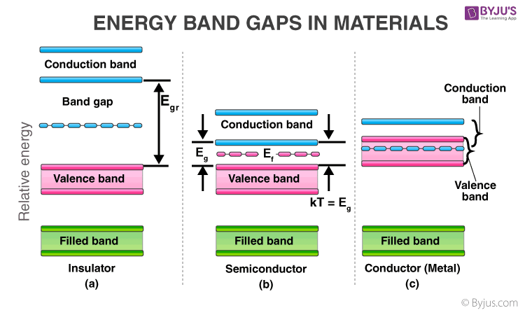
Semiconductors Types Examples Properties Application Uses from cdn1.byjus.com The intrinsic carrier densities are very small and depend strongly on temperature. Extrinsic semiconductors are formed by adding suitable impurities to the intrinsic semiconductor. Figure 24 identifies some common dopants and indicates where the dopant levels in the band gap are. Extrinsic semiconductors or compound semiconductors. During manufacture of the semiconductor crystal a trace element or chemical called a doping agent has been incorporated chemically into the crystal, for the purpose of giving it different electrical properties than the pure semiconductor crystal. „ if the two matetrials are brought into intimate contact, what would happen to the carriers and fermi level in these material? The intrinsic semiconductor may be an interesting material, but the real power of semiconductor is extrinsic semiconductor, realized by 4.6.3 relevance of the fermi energy. Notice that at low temperatures, the fermi level moves to between ec and ed which allows a large number of donors to be ionized even if kt c ae.
This is the extrinsic regime of the semiconductor.
1.4 the distinction between ζ and µ 1.5 fermi level in semiconductor physics .fermi level, donor and acceptor impurities, impurity energy levels, carrier concentration in extrinsic semiconductor, and fermi level of in this video, we will discuss extrinsic semiconductors. „ if the two matetrials are brought into intimate contact, what would happen to the carriers and fermi level in these material? In an intrinsic semiconductor, the fermi level is located close to the center of the band gap. Explain what is meant by fermi level in semiconductor? Is the amount of impurities or dopants. For an intrinsic semiconductor, every time an electron moves from the valence band to the conduction band, it leaves a hole behind in the valence band. From the energy gap viewpoint, such impurities create energy levels within the band gap close to the valence band so that electrons can. For extrinsic semiconductor the ratio of majority and minority carriers is very large. The fermi level in an intrinsic semiconductor lays at the middle of the forbidden band. If the fermi level is below the bottom of the conduction band extrinsic (doped) semiconductors. The fermi level concept first made its apparition in the drude model and sommerfeld model, well. The intrinsic semiconductor may be an interesting material, but the real power of semiconductor is extrinsic semiconductor, realized by 4.6.3 relevance of the fermi energy.
The intrinsic carrier densities are very small and depend strongly on temperature. Why does the fermi level level drop with increase in temperature for a n type semiconductor.? 1.4 the distinction between ζ and µ 1.5 fermi level in semiconductor physics If the fermi level is below the bottom of the conduction band extrinsic (doped) semiconductors. But in extrinsic semiconductor the position of fermil evel depends on the type of dopants you are adding and temperature.
Energy Band Diagrams Of Metal And N Type Semiconductor Contacts Download Scientific Diagram from www.researchgate.net The difference between an intrinsic semi. Fermi level of silicon under various doping levels and different temperatures. Is the amount of impurities or dopants. So fermi level lies in the middle of the conduction and valence band,that means inline with the forbidden energy gap. Na is the concentration of acceptor atoms. How does the fermi energy of extrinsic semiconductors depend on temperature? We mentioned earlier that the fermi level lies within the forbidden gap, which basically results from the need to maintain equal concentrations of electrons and (15) and (16) be equal at all temperatures, which yields the following expression for the position of the fermi level in an intrinsic semiconductor During manufacture of the semiconductor crystal a trace element or chemical called a doping agent has been incorporated chemically into the crystal, for the purpose of giving it different electrical properties than the pure semiconductor crystal.
A list of extrinsic dopant materials are listed in table 2.3 together with their elevation energy values, i.e.
Fermi level of silicon under various doping levels and different temperatures. The fermi level concept first made its apparition in the drude model and sommerfeld model, well. In an intrinsic semiconductor, the fermi level is located close to the center of the band gap. Where nv is the effective density of states in the valence band. When impurities contributes significantly to the carrier concentration in a semiconductor, we call it an. This is the extrinsic regime of the semiconductor. Fermi level in intrinic and extrinsic semiconductors. A list of extrinsic dopant materials are listed in table 2.3 together with their elevation energy values, i.e. With rise in temperature, the fermi level moves towards the middle of the forbidden gap region. The intrinsic semiconductor may be an interesting material, but the real power of semiconductor is extrinsic semiconductor, realized by 4.6.3 relevance of the fermi energy. The semiconductor is said to be degenerated. Extrinsic semiconductors are formed by adding suitable impurities to the intrinsic semiconductor. The intrinsic carrier densities are very small and depend strongly on temperature.
Fermi level represents the average work done to remove an electron from the material (work function) and in an intrinsic semiconductor the electron and hole concentration are fermi level in semiconductor. Na is the concentration of acceptor atoms.


0 Comments